Circuit Board Drawing
Circuit Board Drawing - Web to design a printed circuit board (pcb), you need to draw holes, pads, and wires for your circuit. Electrical components are identified two main ways. Pcb design is usually done by converting your circuit’s schematic diagram into a pcb layout using pcb layout software. To learn how to begin your pcb design journey, see how to become a pcb designer. After seeing a few circuit diagrams, you’ll quickly learn how to distinguish the different symbols. Start by finding the schematics for your diagrams and draw holes, wires, and pads for the circuit. Printed circuit board design in 10 steps. Your choice will usually be based on the availability of materials needed by the method, the technical difficulty level of the method or the quality of pcb you desire to obtain. And we will look at how to read pcb schematics in this article to get you. Web a circuit diagram, or a schematic diagram, is a technical drawing of how to connect electronic components to get a certain function.
The typical size is usually 3.5 inches (8.9 cm) by 5 inches (12.7 cm). This software just lets you develop electronics the right way. This tutorial should turn you into a fully literate schematic reader! Web in this kicad tutorial for beginners, you'll learn to make your first printed circuit board (pcb). Web a circuit diagram, or a schematic diagram, is a technical drawing of how to connect electronic components to get a certain function. Choose a method to use for creating the pcb. 10 simple steps to learn electronics. Designing a circuit schematic in. A ruler is also helpful. Schematics are our map to designing, building, and troubleshooting circuits.
The tool includes a comprehensive electronic symbol library and an integrated digikey component catalog that allows for a. The typical size is usually 3.5 inches (8.9 cm) by 5 inches (12.7 cm). The next thing that should be done is to prepare the board layout. Web a pcb schematic is a circuit diagram designers use in the first stage of the board design process. Each electronic component has a symbol. To learn how to begin your pcb design journey, see how to become a pcb designer. Web circuit diagram is a free application for making electronic circuit diagrams and exporting them as images. Pcb design is usually done by converting your circuit’s schematic diagram into a pcb layout using pcb layout software. A ruler is also helpful. Understanding how to read and follow schematics is an important skill for any electronics engineer.

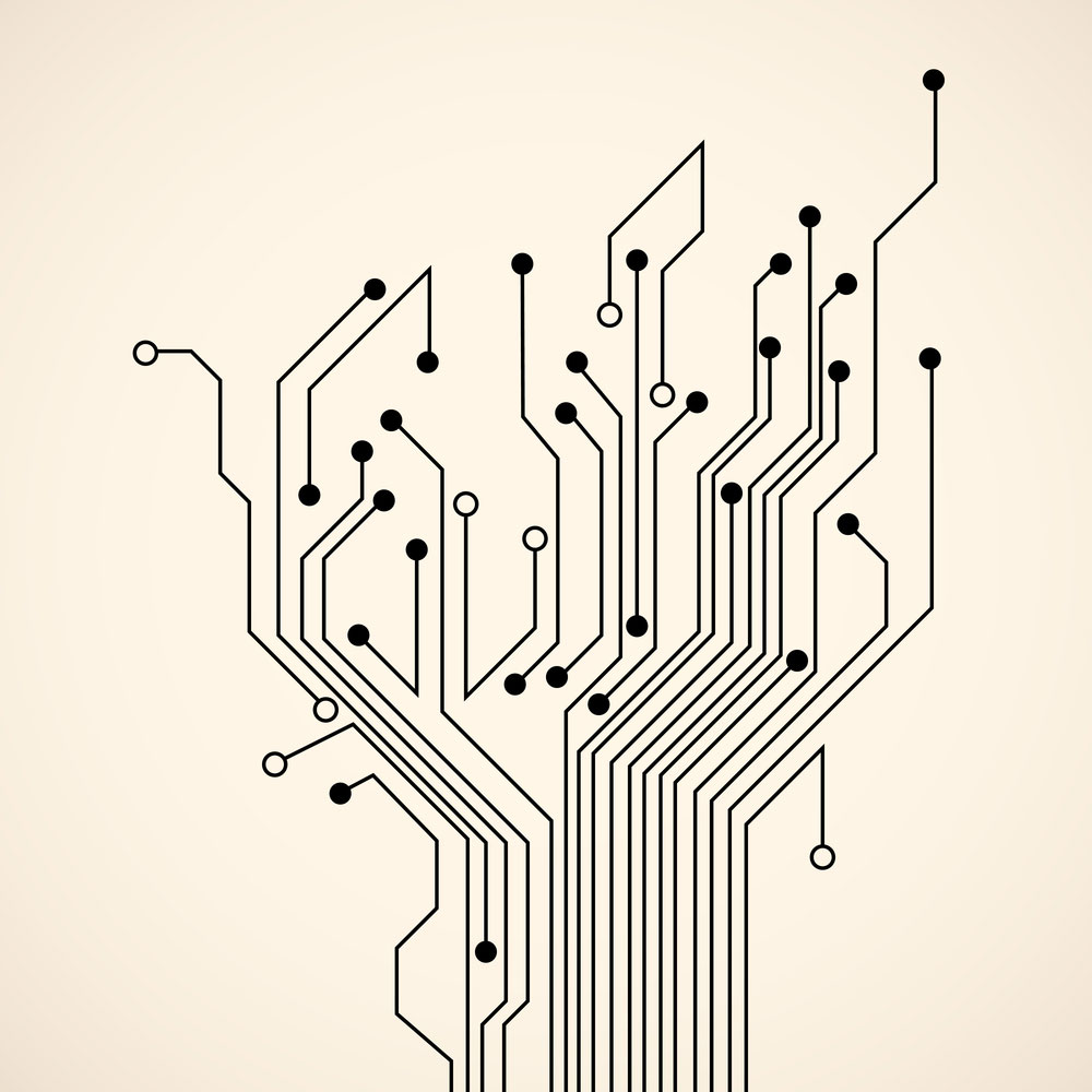
Hand draw computer circuit board on paper Vector Image
Official guide to tinkercad circuits. Understanding how to read and follow schematics is an important skill for any electronics engineer. The tool includes a comprehensive electronic symbol library and an integrated digikey component catalog that allows for a. Web a printed circuit board is a bunch of electronic components interconnected via conductive paths printed on a baseboard. To learn how.
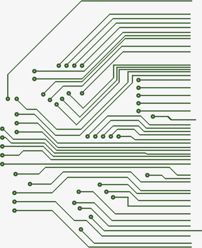
Circuit Board Drawing at GetDrawings Free download
Web easyeda is a free and easy to use circuit design, circuit simulator and pcb design that runs in your web browser. It would help if you then drew your schematic into the software chosen. We'll go over all of the fundamental schematic symbols: A circuit diagram is a diagram showing and explaining how and where electronic components will be.
Circuit Board Drawing at GetDrawings Free download
Schematics are our map to designing, building, and troubleshooting circuits. A pcb schematic is a logical and visual representation of an electrical circuit. Each electronic component has a symbol. This software just lets you develop electronics the right way. Professional schematic pdfs, wiring diagrams, and plots.
How To Create A Simple Circuit Board Drawing
Choose a method to use for creating the pcb. 10 simple steps to learn electronics. A pcb schematic is a logical and visual representation of an electrical circuit. Start by finding the schematics for your diagrams and draw holes, wires, and pads for the circuit. Web in this kicad tutorial for beginners, you'll learn to make your first printed circuit.
How To Create A Simple Circuit Board Drawing
One of the key concepts in electronics is the printed circuit board or pcb. Professional schematic pdfs, wiring diagrams, and plots. And we will look at how to read pcb schematics in this article to get you. Web simple circuit board drawing — where does one need to start. A pcb schematic is a logical and visual representation of an.
Circuit Board Drawing at Explore collection of
Web acquire a circuit board. Web to design a printed circuit board (pcb), you need to draw holes, pads, and wires for your circuit. Web simple circuit board drawing — where does one need to start. Seamless circuit design for your project. The typical size is usually 3.5 inches (8.9 cm) by 5 inches (12.7 cm).

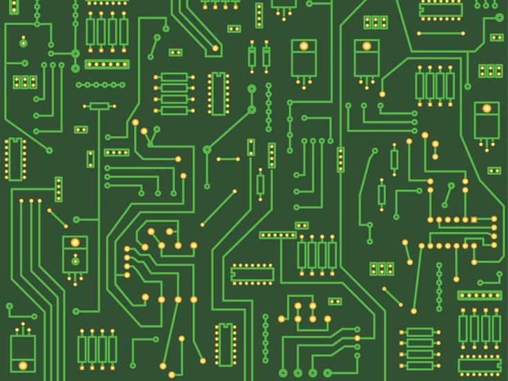
Circuit Board Vector Art, Icons, and Graphics for Free Download
After seeing a few circuit diagrams, you’ll quickly learn how to distinguish the different symbols. Tinkercad circuits is the easiest way to get students started with electronics—available on any computer. So knowing these schematics is paramount. And we will look at how to read pcb schematics in this article to get you. Web create a blank pcb layout.
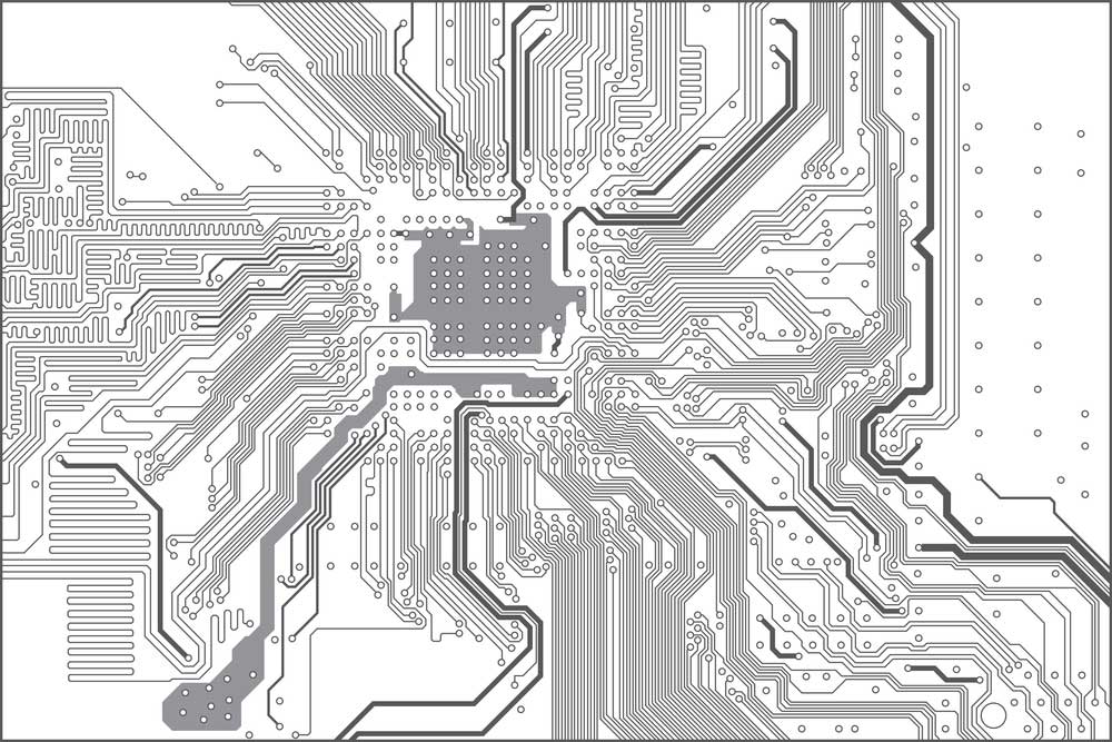
printed circuit board drawing Wiring Diagram and Schematics
Circuit boards are about a dollar apiece, and are simply a layer of copper over an insulator. Web 9:00 am to 4:00 pm pt. Electrical components are identified two main ways. A pcb schematic is a logical and visual representation of an electrical circuit. A ruler is also helpful.
Circuit Board Drawing at GetDrawings Free download
The next thing that should be done is to prepare the board layout. Web acquire a circuit board. Web it involves setting up the board parameters, determining its outline, routing the components, and generating the production documents by adhering to a suitable design checklist. Your choice will usually be based on the availability of materials needed by the method, the.
Circuit Board Drawing at Explore collection of
In this instructable i will talk about how to read a schematic and how to identify electrical components on a pcb (printed circuit board). Web acquire a circuit board. Circuit boards are about a dollar apiece, and are simply a layer of copper over an insulator. Seamless circuit design for your project. Printed circuit board design in 10 steps.
Your Choice Will Usually Be Based On The Availability Of Materials Needed By The Method, The Technical Difficulty Level Of The Method Or The Quality Of Pcb You Desire To Obtain.
Choose a method to use for creating the pcb. 10 simple steps to learn electronics. Web easyeda is a free and easy to use circuit design, circuit simulator and pcb design that runs in your web browser. A pcb schematic is a logical and visual representation of an electrical circuit.
Electrical Components Are Identified Two Main Ways.
The tool includes a comprehensive electronic symbol library and an integrated digikey component catalog that allows for a. It's so fundamental that people often forget to explain what a pcb is. Web it involves setting up the board parameters, determining its outline, routing the components, and generating the production documents by adhering to a suitable design checklist. Web circuit diagram is a free application for making electronic circuit diagrams and exporting them as images.
Web Create A Blank Pcb Layout.
To learn how to begin your pcb design journey, see how to become a pcb designer. The next thing that should be done is to prepare the board layout. In this instructable i will talk about how to read a schematic and how to identify electrical components on a pcb (printed circuit board). Design circuits online in your browser or using the desktop application.
Defining Design Rules And Dfm Requirements.
Circuit boards are about a dollar apiece, and are simply a layer of copper over an insulator. The electronic components and conductive paths are based on a map, the schematic diagram. And we will look at how to read pcb schematics in this article to get you. Analog & digital circuit simulations in seconds.